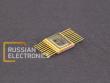
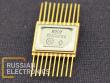
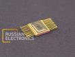
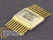
8-bit register with Z-state based on latch triggers designed to control high-capacity and low-resistance load.
Terminal assignment:
1 – high impedance state input
2 – Q0 output
2 – D0 input (data)
4 – D1 input (data)
5 – Q1 output
6 – Q2 output
7 – D2 input (data)
8 – D3 input (data)
9 – Q3 output
10 – common terminal
11 – C input (clock)
12 – Q4 output
13 – D4 input (data)
14 – D5 input (data)
15 – Q5 output
16 – Q6 output
17 – D6 input (data)
18 – D7 input
19 – Q7 output
20 – power supply
Truth table
| Input | Output | ||
| __ EZ | C | D | Q |
| 0 | 1 | 1 | 1 |
| 0 | 1 | 0 | 0 |
| 0 | 0 | X | Q0 |
| 1 | X | X | Z |
Electrical parameters
| Rated power supply voltage, V | 5±10% |
| Low-level output voltage, V at I0OUT=12 mA at I0OUT=24mA | ≤0.4 ≤0.5 |
| High-level output voltage, V at I1OUT=-2.6mA at I1OUT=-0.4mA | ≥2.4 ≥2.5 |
| Forward voltage drop at clamp diode, V | ≤|-1.5| |
| Current consumption at low-level input voltage at US=5.5 V, mA | ≤25 |
| Current consumption at high-level input voltage at US=5.5 V, mA | ≤16 |
| Current consumption in off-state at US=5.5 V, UOUT=2.7 V, mA | ≤27 |
| Low-level input current, mA | ≤|-0.1| |
| High-level input current, µA | ≤20 |
| Disruptive input current, mA | ≤0.1 |
| Output current, mA | |-30|..|-112| |
| Off-state high-level output current, µA | ≤20 |
| Off-state low-level output current, µA | ≤|-20| |
| Turn-on propagation delay time, ns D input C input | ≤16 ≤23 |
| Turn-off propagation delay time, ns D input C input | ≤12 ≤22 |
| Off-state to high-level propagation delay time, ns | ≤20 |
| High-level to off-state propagation delay time, ns | ≤40 |
| Off-state to low-level propagation delay time, ns | ≤18 |
| Low-level to off-state propagation delay time, ns | ≤30 |
| Input capacitance, pF | ≤5 |
| Output capacitance, pF | ≤7 |
Operational limits
| Power supply voltage, V | 4.5..5.5 |
| Low-level input voltage, V | 0..0.8 |
| High-level input voltage, V | 2..5.5 |
| Maximum input voltage, V | 5.5 |
| Ambient air temperature, oC | -10..+70 |