Universal voltage comparators 521СА3, 521СА301, Р554СА3А, Б521СА3-1, Н521СА3, К521СА301, К554СА301 and К554СА3 are general purpose voltage comparators (VC) with low input current and a wide input voltage range. They can work with a unipolar power supply as well, e.g. +5 V or -30 V. The comparator has two outputs: open collector and emitter. In this case the load can be connected to ground, and positive or negative supply rails. VCs are designed to be used in a wide range of applications.
| Type of product | Specification Number | Type of package |
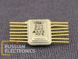
| 521СА301 | бК0.347.015 ТУ2 | 3101.8-1 |
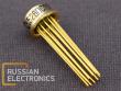
| 521СА3 | бК0.347.015 ТУ2 | 301.8-2 |
| Р554СА3А | бК0.347.473-02 ТУ | 2101.8-1 |
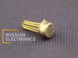
| Б521СА3-1 | бК0.347.115 ТУ2 | no package |
| Н521СА3 | бК0.347.015 ТУ2 | Н04.16-2В |
| К521СА301А,Б | бК0.348.279-02 ТУ | 3101.8-1 |
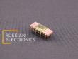
| К554СА3А,Б | бК0.348.279-02 ТУ | 201.14-1 |
| К554СА301А,Б | бК0.348.279-02 ТУ | 2101.8-1 |
Pin Assignement Table
| Pin number, type of package | Symbol | Parameter | |||
| 3101.8-1/301.8-2 no package (flex. output) | Н04.16-2В | 2101.8-1 | 201.14-1 | ||
| 1 | 4 | 1 | 2 | COM | Emitter output |
| 2 | 5 | 2 | 3 | +IN | Non-inverting input terminal |
| 3 | 6 | 3 | 4 | -IN | Inverting input terminal |
| 4 | 1 | 4 | 6 | V- | Voltage UCC2 (-15 В) |
| 5 | 9 | 5 | 7 | BAL | Balancing |
| 6 | 12 | 6 | 8 | BAL/STR | Balancing, gating |
| 7 | 13 | 7 | 9 | OUT | Collector output |
| 8 | 1 | 8 | 11 | V+ | Voltage UCC1 (+) |
Basic Electrical Parameters for the Temperature Range: 0оС ÷ 70 оС
| Parameter, unit | Symbol | Design Ratio | Notes | |||||||||
| 521СА3 521СА301 | Р521СА3А Н521СА3 | Б521СА3-1 | К521СА301А К554СА3А | К521СА301Б К554СА3Б | ||||||||
| min | max | min | max | min | max | min | max | min | max | |||
| Zero offset voltage, mV (UCC12= ±15 V, RG=50k) | UIO | -3 | 3 | -3 | 3 | -3 | 3 | -3 | 3 | -7,5 | 7,5 | |
| Residual voltage, V (UCC= ±15 V,UI= 0,01 V, IL=50 mA) | USAT | - | 1,5 | - | 1,5 | - | 1,5 | - | 1,5 | - | 1,5 | |
| Average input current, nA (UCC1= 15 V,UCC2= -15 V) | I I | - | 100 | - | 100 | - | 100 | - | 100 | - | 250 | |
| Differential input current, nA (UCC1= 15 V,UCC2= -15 V) | IIО | - | 10 | - | 10 | - | 10 | - | 10 | - | 50 | |
| Voltage gain (UCC= ±15 V, UО= ± 10 V, RH = 10k ) | AU | 150k | - | 150k | - | 150k | - | 150k | - | 150k | - | |
| Positive power source current, mA (UCC= ±15 V,UI= 0,01 V) | ICC1 | - | 6 | - | 6 | - | 6 | - | 6 | - | 7,5 | |
| Negative power source current, mA (UCC= ±15 V,UI= 0,01 V) | ICC2 | - | 5 | - | 5 | - | 5 | - | 5 | - | 5 | |
| Dealy time, ns (UCC1= 15 V,UCC2= -15 V, UAC=5 mV) | t DLH | - | 300 | - | 300 | - | 300 | - | 300 | - | 370 | |
| Ultimate and Limit Load Operation Ranges | ||||||
| Parameter, unit | Symbol | Design Ratio | Limit load operation time, max | |||
| Ultimate Load | Limit Load | |||||
| min | max | min | max | |||
| Positive power supply voltage, V | UCC1 | 13,5 | 15,5 | 11,0 | 17,0 | 2 hours |
| Negative power supply voltage, V | UCC2 | -16,5 | -13,5 | -17,0 | -11,0 | |
| Common-mode input voltage, V at UCC= ±16,5 V | UIC | -15,0 | 15,0 | -15,2 | 15,2 | |
| Input Voltage, V | UI | - | 30* | - | 30,1* | |
| Voltage between pin 8(1) and 4(8), V | - | 27 | 33 | 4,5 | 33,4 | |
| Voltage between pin 7(13) and 1(4), V | - | - | 33 | - | 33,4 | |
| Notes: * Absolute values of voltage at the microcircuits input terminals shall not exceed absolute values of power supply voltage. Common-mode input voltage values are given for the power supply UCC=±16,5 V. Comparator dissipated power shall not exceed 500mW. Dissipated power at ambient temperature above 75ОС is calculated according to the gollowing formula: PTOT=500 – (tamb - 75ОС)/ RTh-r, где RTh-r=0,17ОС /mW - thermal rsistance (crystal - amb. medium). | ||||||