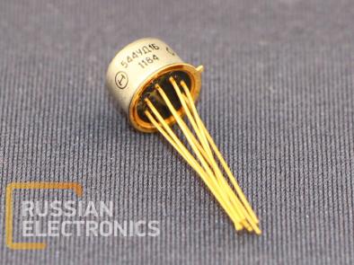
544UD1B
Operational difference amplifier with high input resistance, low level of input current, built-in frequency compensation, allowing the usage with all modes of negative feedback, including integrator and voltage repeater modes. The complex of characteristics allows this IC to be used instead of other operational amplifiers, as well as an integrator with long integration time and high accuracy, in electrometers and logarithmic amplifiers with extended logarithmation range. Low noise current and good noise voltage spectrum characteristics allows to use the amplifier for high-resistance photoelectric receivers with current-to-voltage conversion, sample-and-hold circuits and high-resistance buffers.
Main parameters
| Rated power supply voltage, V | ±15±10% |
| Secondary power supply voltage, V | ±7..±16.5 |
| Current consumption, not more than, A | ±3 |
| Maximum output voltage, V | ±10 |
| Maximum common-mode output voltage, V | ±12 |
| Minimum load resistance, K? | 2 (limit 1) |
| Maximum load capacitance, pF | 500 |
| Equivalent input noise voltage, µV | <5 |
| Zero point offset voltage, mV | ±20 |
| Zero point offset voltagetemperature drift, nV/oC | <25 |
| Input current, not more than, nA | 0.05 |
| Input current difference, not more than, nA | 0.02 |
| Voltage gain ratio | >200000 |
| Common-mode rejection ratio, dB | >80 |
| Power supply voltage impact on zero point offset voltage, µV/V | <100 |
| Input resistance, ? | >1.5?1011 |
| Gain-crossover frequency, MHz | >1 |
| Maximum slew rate, V/µs | >5 |
| Ambient air temperature, oC | -45..+70 |
| Case type | 3101.8-8.01 |


