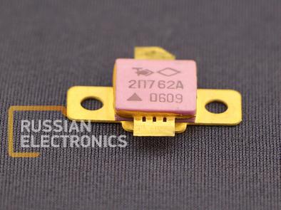
Epitaxial-planar silicon insulated-gate switching FET with n-channel for use in key stabilizers, impulse power supply modulators, electric drive, control and switching circuits.
Case type: metal-ceramic with strip terminals
Mass not more than 5g
Electrical parameters
| Drain-to-source resistance in on-state at UGD=15 V and ID=30 A, ? | 0.075*..0.08*..0.085 |
| Initial drain current at UDS=max, UGD=0 V, not more than, mA at +25 oC, -60 oC at +125 oC | 2 8 |
| Gate leakage current at UGD=15 V, not more than, A | 2.5?10-7 |
| Threshold voltage at UDS=10 V and ID=10mA, V | 2..5 |
| Turn-on time at US=50 V, UINP=10 V, RG=3 ?, RL=2 ?, bogey value, ns | 40* |
| Turn-off time at US=50 V, UINP=10 V, RG=3 ?, RL=2 ?, bogey value, ns | 80 |
| Input capacitance at UDS=20 V, UGD=0 V, pF | 2800*..3000*..3330* |
| Input-to-output capacitance at at UDS=20 V, UGD=0 V, pF | 170*..210*..240* |
| Output capacitance at at UDS=20 V, UGD=0 V, pF | 570*..600*..650* |
Operational limits
| Drain-to-source voltage, V | 100 |
| Gate-to-drain voltage, V | 15 |
| Gate-to-source voltage, V | 100 |
| Drain current (continuous), A | 30 |
| Drain current (impulse), A | 100 |
| Power dissipation at -60..+35 oC, W | 80 |
| Junction temperature, oC | +150 |
| Ambient air temperature, oC | -60..+125 |
At case temperature more than +35 oC power dissipation equals formula Pmax=(150-TC)/RT(P-C)
Mounting method: soldering, not more than 3 times. Minimum distance from case till terminal bend 3mm. Minimum distance from case to soldering point 3 mm, temperature not more than +265 oC, soldering duration 3 s.
Thermal interface roughness 1.6 µm, variation in plane not more than 0.02 mm. Thermal grease usage recommended for contact resistance reduction.


